| View previous topic :: View next topic |
| Author |
Message |
McZonk
Joined: 14 Jul 2005
Posts: 35
Location: Germany
|
 Posted: Sat Dec 03, 2005 9:58 pm Post subject: PSP Flash Chip Facts: The Good, the Bad and the Ugly Posted: Sat Dec 03, 2005 9:58 pm Post subject: PSP Flash Chip Facts: The Good, the Bad and the Ugly |
 |
|

With the help of some university lecturer I have removed the flash chip from a psp board. Neither the board nor the chip are damaged. My idea is to build a PSP with 2 flash roms. If I brick one, I can restore it with other one. Everybody how has a bricked PSP can help Team Emergency Exit with giving us the board. I also need some money for build a circuit board to attach two on. Contact: mczonk@teamemergencyexit.com
The Good Facts
The chip is a standard chip from Samsung: K5E5658HCM . There is nothing secret with the chip. Everybody can buy it, if you take 1000 :D
The Bad Facts
The chip is not only the flash rom (256 mbit nand rom). It is also the ram (256 mbit ddr ram). If you read though the datasheets of the chip, you will find there figures. The flash is built from nand gates. It won't be as easy as access nor gates. So direcly writing into the flash is not easy.
The Ugly Facts
If you look at the board, you will see the wire loops from processor to the flash/ram chip. These wires are made to keep all wires in the same length. This is important for the timing of the ram and timing is very very cirical. If I brought back the flash/ram on the board with just some small wire brigdes, it could disturb the timing of the ram. The flash is not critical, but the ram is.
I will also try to build a two flash psp. |
|
| Back to top |
|
 |
Rich43
Joined: 22 Oct 2005
Posts: 28
|
| Posted: Sat Dec 03, 2005 11:36 pm Post subject: |
|
|
| keep up the good work, bet u will be turning 2.5's into 1.5 in no time :) |
|
| Back to top |
|
|
mrbrown
Joined: 17 Jan 2004
Posts: 1536
|
| Posted: Sun Dec 04, 2005 12:47 am Post subject: |
|
|
The Good News and the Bad News
The Bad News: Nem pulled off his flash chip back in April. He built an interface to flash his PSP externally. He used this interface to deliver the first legitimate homebrew program for PSP and as a method of infilitrating kernel mode. We've known about the identity of the flash chip since before then.
The Good News: Using forum search will help you find this useful information in the future (and perhaps save you a PSP) :). |
|
| Back to top |
|
|
Dr. Vegetable
Joined: 14 Nov 2005
Posts: 171
Location: Boston, Massachusetts
|
| Posted: Sun Dec 04, 2005 4:52 am Post subject: |
|
|
It looks like that thread was not the one you intended to link. But thanks to the forum search tip, I found the relevant topic:
http://forums.ps2dev.org/viewtopic.php?t=1599
(Edited to filter some of my foul attitude. Sorry, mrbrown, I was feeling a bit cranky when I originally posted.)
Last edited by Dr. Vegetable on Mon Dec 05, 2005 1:38 am; edited 1 time in total |
|
| Back to top |
|
|
Pit0711
Joined: 24 Mar 2005
Posts: 54
Location: Old Europe -Germany-
|
| Posted: Sun Dec 04, 2005 8:05 am Post subject: |
|
|
better go to iraq, cowboys
germany over all :-) |
|
| Back to top |
|
|
Dr. Vegetable
Joined: 14 Nov 2005
Posts: 171
Location: Boston, Massachusetts
|
| Posted: Mon Dec 05, 2005 1:34 am Post subject: |
|
|
So I am wondering about the availability of this part. Like others, I have found it listed in Samsung product selection guides, but have not found a datasheet. Pinouts for similar chips do not match either the pad footprint or the apparent wiring to this chip. I've even read claims that Samsung has refused to provide information about this chip because they are bound by an NDA with Sony.
Has anyone had any success mapping the pinout? (Nem apparently has some information, since he has dumped the firmware out of one.) Anyone care to share what they have learned so far?
EDIT:
@Pit0711: Please stay on topic. :)
OK, me first...
Here are my notes from examining a PSP that had suffered a similar fate as the one pictured above. This is the pad layout on the PCB, in the PSP's natural orientation, with the main processor off to the left:
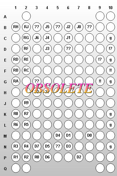
The key to these pin descriptions is as follows:
R0...RH - Nineteen tuned-path traces leading over to the main processor. These appear to be address/control lines?
D0...D7 - 8-bit bus that leads from main processor, past button-cell and up from below (south of) the NAND chip.This could be an 8-bit data bus?
J0...J6 - 7-bit bus emerging from VIAs near button cell, leading around to the north side of the NAND chip. This could be the re-flashing control lines?
?? - Indicates a pin that is connected by a trace to a VIA beneath the NAND.
!! - Indicates a pin that is connected to a diagonal neighbor by a trace beneath the NAND chip.
!? - Indicates a pin that is connected to a diagonal neighbor by a trace beneath the NAND chip which also has a VIA.
g - Indicates pins that are connected directly to the ground plane.
I have not yet determined where all of the VIAs lead, but it appears that some of these do not go all the way through all layers of the PCB. It also is possible that many other pins are connected directly to other layers through VIAs at the pad itself. I have a few other ambiguous notations on some other pins, so I'll have to remind myself by looking at the board again.
I would like to refine this diagram using whatever information anyone would care to submit. This would include any solid information about the purpose of the various bus groups that I have tentatively identified, above. |
|
| Back to top |
|
|
Dr. Vegetable
Joined: 14 Nov 2005
Posts: 171
Location: Boston, Massachusetts
|
| Posted: Tue Dec 06, 2005 1:17 pm Post subject: |
|
|
| More of the pieces are falling into place regarding the NAND chip pinout. Does anybody care, or am I just wasting my time to post documentation on this? |
|
| Back to top |
|
|
faldore
Joined: 05 Dec 2005
Posts: 3
|
|
| Back to top |
|
|
groepaz

Joined: 01 Sep 2005
Posts: 305
|
|
| Back to top |
|
|
DigitalFoundry
Joined: 20 Jan 2005
Posts: 47
|
| Posted: Tue Dec 06, 2005 10:17 pm Post subject: |
|
|
As pointed out earlier, it was hardware dissection like this that actually led to the first legimitate homebrew. Surely there is a place here for informed discussion on the hardware, even if it is in the off-topic forum?
The only problem with the two sites you mention is that finding useful information in amongst all the junk is pretty much impossible. |
|
| Back to top |
|
|
ooPo
Site Admin
Joined: 17 Jan 2004
Posts: 2032
Location: Canada
|
| Posted: Wed Dec 07, 2005 3:32 am Post subject: |
|
|
| Moved to PSP hardware Development. |
|
| Back to top |
|
|
Dr. Vegetable
Joined: 14 Nov 2005
Posts: 171
Location: Boston, Massachusetts
|
| Posted: Wed Dec 07, 2005 11:40 pm Post subject: |
|
|
I have added some details to the pinout for the flash chip. I have mainly renamd pins according to the designations used by Samsung, and guessed at the usage of some of the RAM control lines, based on similar usage in other chips.
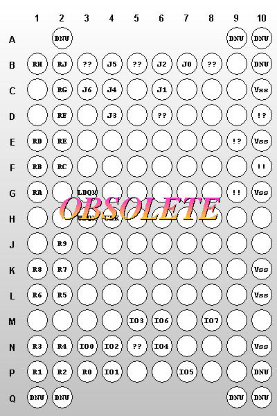
I am in the process of adding the actual traces on the PCB to this diagram in order to help people figure out where they are connected without harming any more PSPs. Since the PSP I am examining suffered some damage duing the extraction process, I am not 100% sure that all traces are still intact.
Also, I believe that the 19 pins in the R0-RJ group are the RAM address lines (there should be 16 of these?) and related control lines. If these pins are organized like other chips, then the low-order address lines are actually at the "RJ" end, not at the "R0" end.
"DNU" means "Do Not Use", which is different than "NC" in that these pins are apparently connected to the wafer and used in the manufacturing/test process for the device. They should not be connected to the circuit. Again, I am guessing at which pins are DNU based on similar designs.
The J0-J6 pin group is most likely the re-flashing control lines. Although I do not yet know which is which, the seven lines available from other chips for this purpose are:
/CE - Chip Enable, active low
R/B - Read/Busy, chip busy writing when low, can be read when high
/RE - Read Enable, active low
/WE - Write enable, active low
/WP - Write Protect, active low
CLE - Command Latch Enable, active high, command provided via IO0...IO7 pins and latched on rising edge of /WE
ALE - Address Latch Enable
I will continue to post updates as I figure out more. I would greatly appreciate any information that others would care to submit in order to verify my findings/guesswork. |
|
| Back to top |
|
|
Shine
Joined: 03 Dec 2004
Posts: 728
Location: Germany
|
| Posted: Thu Dec 08, 2005 12:46 am Post subject: |
|
|
| Dr. Vegetable wrote: |
I will continue to post updates as I figure out more. I would greatly appreciate any information that others would care to submit in order to verify my findings/guesswork. |
I think instead of guessing the right pins it would be easier to just ask nem, because according to http://forums.ps2dev.org/viewtopic.php?p=25484#25484 he has already read the flash chips (and I met him in Amsterdam at the EuroOSCON and he showed his desoldered chips, but not the device he built for reading it :-) |
|
| Back to top |
|
|
Dr. Vegetable
Joined: 14 Nov 2005
Posts: 171
Location: Boston, Massachusetts
|
| Posted: Thu Dec 08, 2005 2:13 am Post subject: |
|
|
I will PM him to make sure he is aware of this thread and to ask for his assistance. Thanks for the tip! I had implied in earlier posts that nem would be a good source for information, but had also wished to solicit help from anyone else who has anything to add.
And I don't plan to base this investigation solely on guessing. I am trying to follow traces back through the PSP circuitry to verify the function of these lines. However, this has to begin with an understanding of what lines are of interest and how they are used.
BTW, it appears that the PSP shares some circuitry between the Memory Stick port and the NAND reflashing circuit. Not at all surprising. But this does imply that the MS slot may provide access to some of the necessary pins without the need to open up the PSP. (Do you see where I am going with this?)
I can certainly hold back on posting this stuff until I have something more solid, if that is preferable. I had just hoped that others who have pursued this line of investigation might jump in and save me some time. |
|
| Back to top |
|
|
nem
Joined: 13 Jan 2005
Posts: 73
|
| Posted: Sun Dec 11, 2005 7:19 pm Post subject: |
|
|
Sorry for late.
Following is a brief memo (could be obsolete partly) for memory chip of PSP, reversed result.
Note that there may be misunderstanding and/or mistakes.
Please confirm yourself before applying hardware hacks for the PSP.
| Code: | SAMSUNG MCP memory chip pinout, flash related
(Top view)
NC NC NC NC
NC GND Vdd 53 Vss NC 52 01 02 03
GND Vdd NC NC 54 Vcc 36 51 05 04
Vdd GND 55 NC 56 64 NC NC GND Vdd
GND Vdd 40 39 34 35 65 NC 06 07
GND Vdd 33 38 37 31 NC NC 08 09
Vdd GND 32 70 67 66 42 NC 10 GND
Vdd GND NC 20 69 68 29 24 21 Vdd
GND Vdd NC 50 41 43 25 27 22 11--------
Vdd GND 45 72 48 30 26 NC 13 12--------
-----------
GND Vdd NC NC 44 46 28 NC 15 14--------
-----+
Vdd GND 71 75 73 47 61 NC 16 Vdd +
-----+ +
GND Vdd 49 74 58 Vss 60 57 17 GND + +--
-----+ +----
NC GND Vdd 63 62 Vcc 59 23 19 18 +---
NC NC NC
<1pin mark here>
Vss Power ground for flash chip
Vcc +3.3V power for flash chip
36 D0
52 D1
51 D2
64 D3
53 D4
56 D5
54 D6
55 D7
58 ~CE
63 ~RE
62 ~WE
59 CLE
60 ALE
57 ~WP
61 R/~B
others: for DRAM
NB:numbers is only for work. no meanings.
|
Access protocol for flash chip is basically same as SAMSUNG's ordinal chip like K9F5608U0C but there exist difference.
Block address should be specified as 3byte length. After writing 1byte command with CLE=H, you must write 4byte address with ALE=H, 3byte block number with 1byte offset within the block. Also you should better to do this sequence not so slowly, or ignored.
Some photos for your interest. Lunar base is the hardware to determine pinouts by bruteforce, and to read the chip.
http://sec.pn.to/pw/?Bases |
|
| Back to top |
|
|
Dr. Vegetable
Joined: 14 Nov 2005
Posts: 171
Location: Boston, Massachusetts
|
| Posted: Sun Dec 11, 2005 8:53 pm Post subject: |
|
|
Thank you for sharing this knowledge with us, nem, you are truly the master!
I will incorporate this information into the diagram I have been putting together, which will become part of a comprehensive online PSP hardware reference that I am assembling. Of course, your groundbreaking contribution will be duly noted. |
|
| Back to top |
|
|
dot_blank

Joined: 28 Sep 2005
Posts: 498
Location: Brasil
|
| Posted: Sun Dec 11, 2005 9:54 pm Post subject: |
|
|
excellent information ;)
your just the person we wanted
to hear from
also what about the possible 7
jtags that run alon right of NAND
and head southeast yet what pinouts
do these 7 end up to ...hmmm ;)
_________________
10011011 00101010 11010111 10001001 10111010 |
|
| Back to top |
|
|
Dr. Vegetable
Joined: 14 Nov 2005
Posts: 171
Location: Boston, Massachusetts
|
| Posted: Mon Dec 12, 2005 3:27 am Post subject: |
|
|
Ok, I finally incorporated nem's notes into my diagram. It was a bit confusing to rotate everything 180 degrees, so I hope I got everything right. I'm not sure that my diagram adds anything new to what nem has posted, but perhaps the layout is a little easier to see this way:
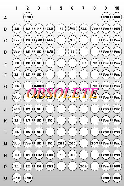
It looks like the only guess I had gotten wrong was to assume that the eight I/O data bus lines would be physically laid out in 0...7 order. (Sneaky Sony!) But these line run into a small network of VIAs near the main processor, so I should have suspected that they were getting swapped around.
dot_blank: You can figure out the mapping of the 7 JTAG lines that run from the button cell to the "southeast" of the NAND chip upward and disappearing beneath the chip from the "north" if you follow my labelling of J0...J6 from right-to-left at the chip's edge:
J0 --> /RE
J1 --> /CE
J2 --> /WE
J3 --> R/B
J4 --> ALE
J5 --> CLE
J6 --> /WP
I am thinking that, if one were to try to use these lines for reflashing, you would also need to provide power to a lot of pins. It seems that a charged battery and/or DC adapter would need to be connected to the PSP with the main processor somehow disconnected or asleep? You would also need to access the IO0...IO7 pins to feed the actual commands, addresses, and data into the chip while flashing.
As I have mentioned in other posts, at least a few of these lines seem to pass through 40-pin connector "CN4201" (north of the NAND chip) and across into the daughterboard. I am patiently ohming this out to see whether there is external access to these lines through the Memory Stick slot and/or the Headphone/SIRCS connector. I am even wondering if there is a way to transfer a firmware image directly from a memory stick onto the NAND chip.
Anyway, a huge thanks to nem for sharing his findings. That probably saved me from bricking quite a few PSPs trying to figure this out for myself. I also must commend his de-soldering skills! He has pictures of a board with both processors and the flash chip lifted that show little if any damage to the PCB. I can only assume that he carefully heated the chips with an iron while gently lifting with an IC puller. My friend's technique of cutting with an exacto blade did not have the same clean results. (Don't try this at home, kids!) |
|
| Back to top |
|
|
pyrosama
Joined: 13 May 2005
Posts: 66
|
| Posted: Mon Dec 12, 2005 4:46 am Post subject: |
|
|
 |
|
| Back to top |
|
|
dot_blank
Joined: 28 Sep 2005
Posts: 498
Location: Brasil
|
| Posted: Mon Dec 12, 2005 4:52 am Post subject: |
|
|
excellent ;)
Dr.V: you might have something
with running something from memstick
to NAND ...really interesting indeed
Pyro: yea thats just what a blind fool
like me needs :P
_________________
10011011 00101010 11010111 10001001 10111010 |
|
| Back to top |
|
|
pyrosama
Joined: 13 May 2005
Posts: 66
|
| Posted: Mon Dec 12, 2005 5:52 am Post subject: |
|
|
| I checked and none of the flash points directly connect to the mobo to dboard connecter. |
|
| Back to top |
|
|
digihoe
Joined: 14 May 2005
Posts: 108
|
| Posted: Mon Dec 12, 2005 9:00 am Post subject: |
|
|
I do think you don't need to worry about the CPU when you are JTAGing the flash (but I can be mistaken this with JTAGing the CPU)...
B.T.W. can you read RAM with this JTAG? Anyone tried reading the flash using this JTAG pins?
Best regards and nice find! |
|
| Back to top |
|
|
Dr. Vegetable
Joined: 14 Nov 2005
Posts: 171
Location: Boston, Massachusetts
|
| Posted: Mon Dec 12, 2005 5:38 pm Post subject: |
|
|
Thanks for checking that out, pyrosama. I would have done this myself, but I've been caring for my 1-year-old son all day. (Tough to get anything constructive done with a little monkey trying to help!) I like your exacto job, too! A bit neater than my friend managed to do, but the scars are all in the same places.
Well, even if no way is discovered to access these pins without opening the PSP, it should be possible to solder some wires onto these seven lines, plus the IO0-IO7 lines, in order to experiment with re-flashing bricked PSPs.
Regarding the CPU vs. JTAG, I'm only worried about the CPU trying to put stuff on the data bus while we're messing with the JTAG port, so I would think the CPU wants to be disabled/suspended. But the chip needs power, so flashing it in-circuit I assume could get interesting. This isn't really a "JTAG" port in the usual sense - it doesn't enable one to take control of the CPU or do single-stepping, reading of registers, etc. These are really just the physical control lines that are used for reading and writing to the non-volatile portion of memory, which contains the firmware and some user settings.
It is possible to read the flash ROM using these pins, as demonstrated by nem. He literally fathered the PSP homebrew movement by reading the 1.0 firmware out of the chip this way. You could theoretically read RAM if you used some of the many other lines going into this chip, but doing so without crashing the machine would be unlikely.
This line of research could lead to a way to bypass the versioning restrictions built into the Sony firmware, allowing us to potentially downgrade any PSP to pretty much any firmware version available. Since there is encryption employed even at this level, we still would lack the ability to install custom firmware unless/until somebody figures out the Sony private keys, which will probably happen about 10,000 years from now.
NOTE TO SONY: (We know you are reading this!) You've built a beautiful machine, here, and I hope you can see the extremes we will go to in order to enable homebrew applications to run on them. I (for one) would like to buy games on UMD to financially support this great platform, but you make it pointless to do so when you force firmware upgrades that are not actually necessary. (Most games run just fine on any version as long as the correct version number is spoofed.)
Why not sell a "Homebrew Developer's Kit" so that your customers can write our own games and applications for this machine? Even if you required people to buy a separate "Homebrew Loader" UMD in order to run these applications, we'd all be able to stop tearing open these beautiful PSPs to perform brain surgery on them.
Please don't fear the Homebrew community; we could be your greatest ally in the game console wars! |
|
| Back to top |
|
|
ryoko_no_usagi

Joined: 29 Nov 2005
Posts: 65
|
| Posted: Mon Dec 12, 2005 5:51 pm Post subject: |
|
|
Um, why are you calling those lines JTAG? They don't look like JTAG to me (although I don't actually know much of JTAG, I just know our hardware guy usually puts a JTAG port on our boards which we use to flash firmware and for debugging...) and I don't think memories themselves usually have JTAG ports?
The point of JTAG is that you can have access to _all_ chips/pins on the board through a simple 4 line serial connection, for verifying PCB or for ISP of flash (through a JTAG capable device connected to the flash, or in my case the MCU usually has built-in flash) or for debugging. If the CPU for instance has a JTAG port, it should be possible to access flash just through the JTAG interface, so no need for connecting to other IO-pins etc. But I don't think the Samsung chip has a direct JAG port so would need to go through another device, and would need to know the format used... |
|
| Back to top |
|
|
Dr. Vegetable
Joined: 14 Nov 2005
Posts: 171
Location: Boston, Massachusetts
|
| Posted: Mon Dec 12, 2005 6:32 pm Post subject: |
|
|
You are correct, these aren't JTAG lines. I've been calling them "JTAG" because that is what they have been called here in the past, probably because they allow one function that is often performed using JTAG.
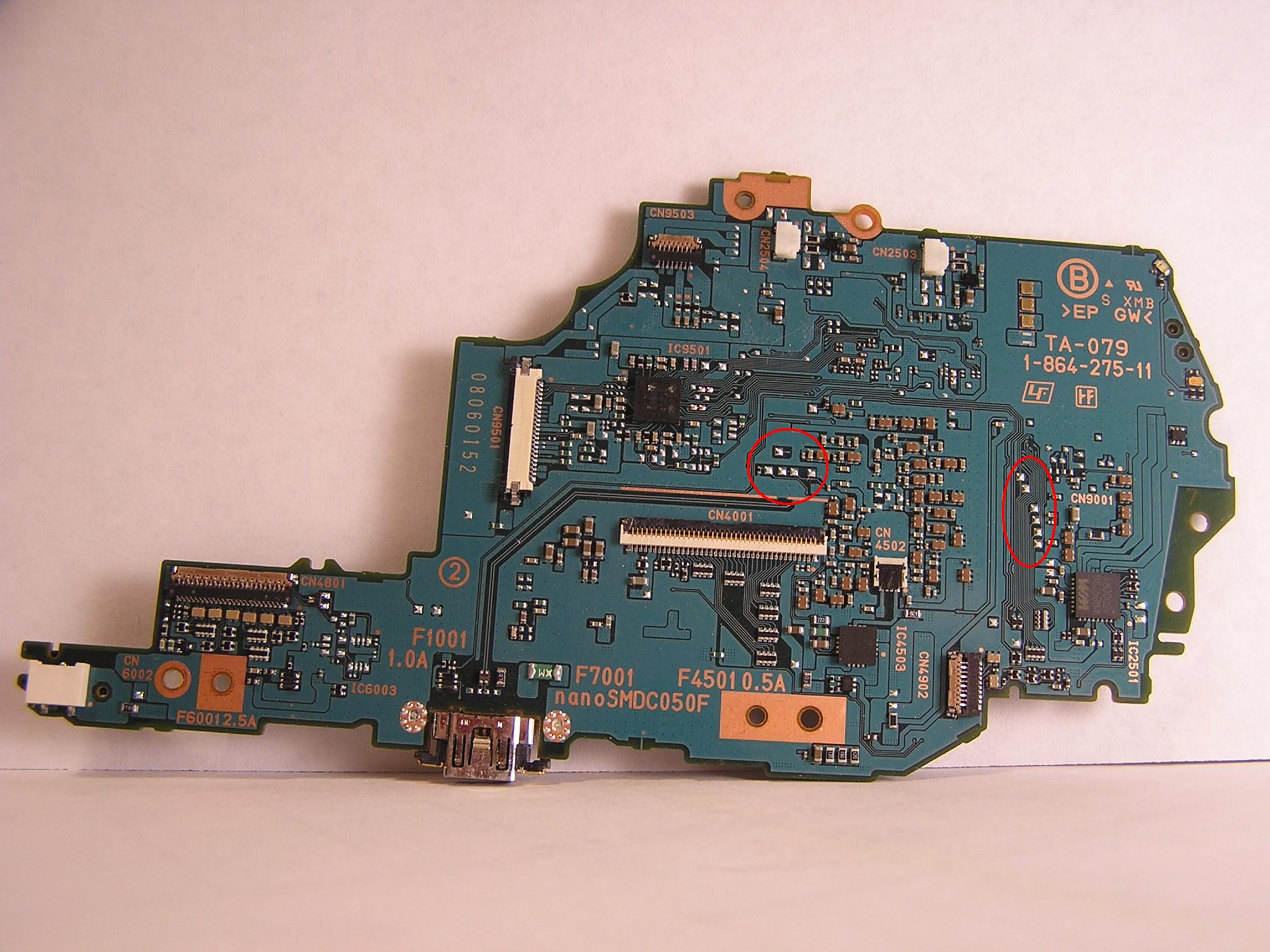
It does make me wonder if there is a real JTAG port in there somewhere... The PSP mainboard has a number of large square solder pads that appear to be test points of some kind. For example, in this picture (original image provided by pyrosama) I have circled two sets of test points:
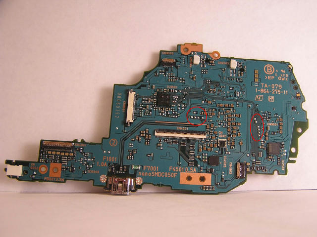
The ones near the center could be the fabled diagnostic COM4 port. (Pure speculation so far.) The ones to the right appear to provide access to the data bus leading to the Memory Stick slot. There are many such pads on the PSP boards (some smaller than these!) that have yet to be explored. |
|
| Back to top |
|
|
pyrosama
Joined: 13 May 2005
Posts: 66
|
| Posted: Mon Dec 12, 2005 6:50 pm Post subject: |
|
|
Those pads from what I can tell dont directly connect to nand but could be jtag. I once talked to a guy who formerly worked for sony on a production line who claimed that the boards were flashed un powered out side of psp through a 7 point jtag that was on the top of the board (under lcd not side with nand)
Though I do not know if there is any truth in what he said.
I poped off my cpu and gpu about 2 hours ago so I will go snap a few shots in a minutes.
As for my realativly clean removal of the chip I used a heat gun prior to atempting to pop of the chip which made it a bit easier.
[edit]
Here are the photos I promised!
Dont say any thing about the location of the nand chip :P
I atempted to remove the solder balls with a butane wood burner (no soldering iron missplaced while moving) so in the proccess I scourched the board!
http://psp.mimimode.net/allboard/cpu/
[/edit]
Canti_ |
|
| Back to top |
|
|
nem
Joined: 13 Jan 2005
Posts: 73
|
| Posted: Tue Dec 13, 2005 1:11 am Post subject: |
|
|
Dr. Vegetable,
You would better to add power pads for flash,
| Code: | Vss Power ground for flash chip
Vcc +3.3V power for flash chip |
GND and Vdd is for DRAM. Vcc(+3.3V) is used for some I/O including daughter board. |
|
| Back to top |
|
|
Dr. Vegetable
Joined: 14 Nov 2005
Posts: 171
Location: Boston, Massachusetts
|
| Posted: Tue Dec 13, 2005 2:05 am Post subject: |
|
|
Ah, thanks for the correction. I will update the diagram to more clearly indicate this distinction. I also plan to color-code the pins to show which are for SDRAM and which are for flash.
Sorry for the confusion! |
|
| Back to top |
|
|
pyrosama
Joined: 13 May 2005
Posts: 66
|
| Posted: Tue Dec 13, 2005 3:19 am Post subject: |
|
|
| Looking good for flashing with out removing chip. Power pins can be accessed easily. |
|
| Back to top |
|
|
Dr. Vegetable
Joined: 14 Nov 2005
Posts: 171
Location: Boston, Massachusetts
|
| Posted: Tue Dec 13, 2005 3:45 am Post subject: |
|
|
Thanks for the new photos! These should really be of interest to a lot of people... Butane torch, eh? Is that where the "pyro" part of your moniker comes from? :)
To Sony: Legitimize Homebrew before another PSP gets whacked! (Maybe we should start mailing the pieces back to them.) |
|
| Back to top |
|
|
|

 FAQ
FAQ Search
 Memberlist
 Usergroups
 Register
 Profile
 Log in to check your private messages
 Log in