| View previous topic :: View next topic |
| Author |
Message |
0okm0000

Joined: 13 Jan 2006
Posts: 116
|
 Posted: Sat Mar 25, 2006 7:28 pm Post subject: Read PSP NAND Flash DATA to PC Posted: Sat Mar 25, 2006 7:28 pm Post subject: Read PSP NAND Flash DATA to PC |
 |
|
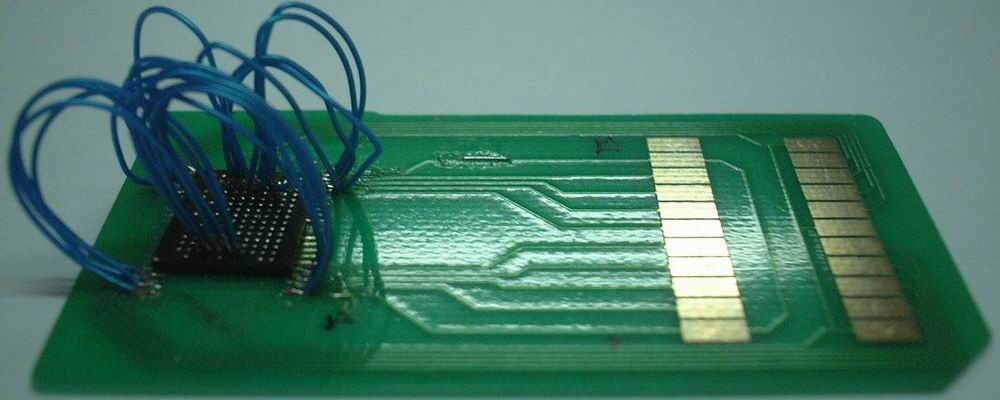
K5E5658HCM-D060 PSP NAND Flash Adaptor
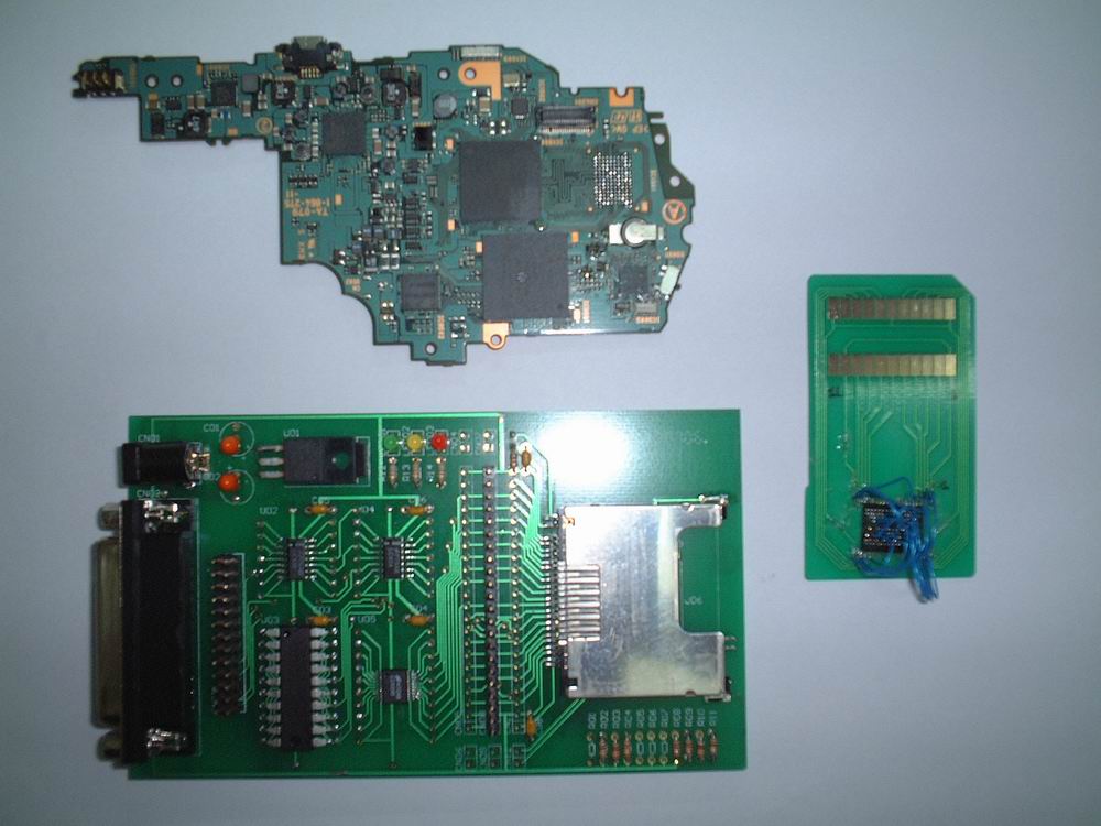
PSP MainBoard, NAND Flash Programer, PSP NAND Flash Adaptor
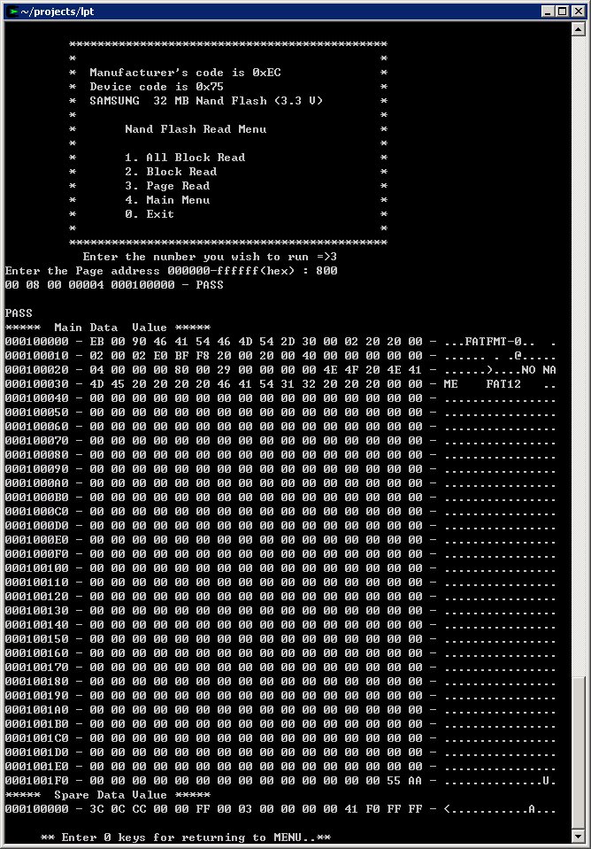
Read PSP NAND Flash DATA to PC |
|
| Back to top |
|
 |
Mathieulh
Joined: 19 Oct 2005
Posts: 68
|
| Posted: Sat Mar 25, 2006 11:47 pm Post subject: |
|
|
nice work :)
I'd be very interested in having the schematics to build those as well as the pinouts used :) |
|
| Back to top |
|
|
HaQue
Joined: 25 Nov 2005
Posts: 91
Location: Adelaide, Australia
|
| Posted: Sun Mar 26, 2006 12:34 pm Post subject: |
|
|
Thats great work, do you have a website anywhere detailing your work? I am interested in the schematics and more information as well as Im sure alot of others are :)
Do you think it is possible to hook it up in circuit?
_________________
www.smartwave-wireless.com |
|
| Back to top |
|
|
ryoko_no_usagi

Joined: 29 Nov 2005
Posts: 65
|
| Posted: Tue Mar 28, 2006 4:13 am Post subject: |
|
|
| To hook it up in-circuit, one would have to find a way to keep the nand-interface in the CPU from hogging the bus. Probably by cutting the traces, which is...messy... |
|
| Back to top |
|
|
Dibblah
Joined: 03 Nov 2005
Posts: 13
|
| Posted: Tue Mar 28, 2006 9:10 am Post subject: |
|
|
| ryoko_no_usagi wrote: | | To hook it up in-circuit, one would have to find a way to keep the nand-interface in the CPU from hogging the bus. Probably by cutting the traces, which is...messy... |
Actually, it may not be as bad as we think, with some hardware purchases:
http://www.stencilsunlimited.com/bga_stencils.php
Then just install a "shim" that pulls out either side of the flash interface (to and from chip). Since you're not changing the different trace-lengths of anything important (it's just the flash lines - The others would need through-holed).
It's a lot of work for DIY, but with the right equipment, it looks easy. |
|
| Back to top |
|
|
Dibblah
Joined: 03 Nov 2005
Posts: 13
|
|
| Back to top |
|
|
0okm0000
Joined: 13 Jan 2006
Posts: 116
|
| Posted: Tue Mar 28, 2006 11:36 am Post subject: |
|
|
the "NAND Flash Programer" was build by me
you can not use CardReader to read NandFlash SpareData & BadBlock
so you need to dev hardware by yourself
or buy the NandFlash devKit/Programer
_________________
PSP hardware hack
http://0okm.blogspot.com/ |
|
| Back to top |
|
|
ryoko_no_usagi
Joined: 29 Nov 2005
Posts: 65
|
| Posted: Tue Mar 28, 2006 3:19 pm Post subject: |
|
|
| Dibblah wrote: | | ryoko_no_usagi wrote: | | To hook it up in-circuit, one would have to find a way to keep the nand-interface in the CPU from hogging the bus. Probably by cutting the traces, which is...messy... |
Actually, it may not be as bad as we think, with some hardware purchases:
http://www.stencilsunlimited.com/bga_stencils.php
Then just install a "shim" that pulls out either side of the flash interface (to and from chip). Since you're not changing the different trace-lengths of anything important (it's just the flash lines - The others would need through-holed).
It's a lot of work for DIY, but with the right equipment, it looks easy. |
Er, I think you misunderstood me. :) That's probably a nice kit for BGA rework, but it is a little overkill for hooking into the nand since all the traces are exposed on the top layer (luck or what?). Probably a lot easier (not to mention cheaper) to just solder wires onto them...
The problem is to keep the CPU off the bus when you want to reflash the nand. It's no good if you have a conflict when you try to assert WE and the CPU want to deassert it for instance :) |
|
| Back to top |
|
|
sea_monster
Joined: 28 Mar 2006
Posts: 7
Location: atlantic
|
| Posted: Tue Mar 28, 2006 5:13 pm Post subject: |
|
|
i would have to agree with Ryoko, the one there who is eating furry ice cream or something.
who cares about soldering to those traces, since those lines are not associated with the crazy fast ram. Problem is, have you SEEN those traces? I was pretty giddy about the via's that almost all the lines ran to. But that was based on photos. Upon seeing an actual board, everything is pretty intimidatingly small.
Anyways, so bring it to work, throw it under a microscope, solder that stuff together... Hook an FPGA up to the lines...
That is all doable, the only question that remains is the CPU right? How to hold it in reset or whatever. Lets figure that out now, and then this job is a wrap!
FYI, Xilinx has a spartan 3 fpga eval board, wicked nice, for only $99, with vhdl synth, full simulation package, programming cable, the outputs can be configured to whatever TTL level you want (up to 3.3V), http://www.xilinx.com/xlnx/xebiz/designResources/ip_product_details.jsp?key=HW-SPAR3-CPLD-DK
i'll do the fpga design (vhdl) if someone else does the rest. |
|
| Back to top |
|
|
Dibblah
Joined: 03 Nov 2005
Posts: 13
|
| Posted: Tue Mar 28, 2006 5:28 pm Post subject: |
|
|
| 0okm0000 wrote: |
the "NAND Flash Programer" was build by me
you can not use CardReader to read NandFlash SpareData & BadBlock
so you need to dev hardware by yourself
or buy the NandFlash devKit/Programer |
True for the USB ones. But not the parallel - All of the smarts there pretty much have to be in the driver... |
|
| Back to top |
|
|
KPOT0B
Joined: 09 Mar 2006
Posts: 9
|
| Posted: Wed Mar 29, 2006 1:25 am Post subject: |
|
|
| Quote: | | It's no good if you have a conflict when you try to assert WE and the CPU want to deassert it for instance :) |
Bet if you will keep reset low the CPU wont even try to do anything and all pins will be in high-z. So you can access Flash that time safely. Probably it possible to make some nail pad which will let you work with Flash chip right on PSP withou soldering :) |
|
| Back to top |
|
|
ryoko_no_usagi
Joined: 29 Nov 2005
Posts: 65
|
| Posted: Wed Mar 29, 2006 6:28 am Post subject: |
|
|
| KPOT0B wrote: | | Quote: | | It's no good if you have a conflict when you try to assert WE and the CPU want to deassert it for instance :) |
Bet if you will keep reset low the CPU wont even try to do anything and all pins will be in high-z. |
Great...so where's the reset? :)
| sea_monster wrote: |
i would have to agree with Ryoko, the one there who is eating furry ice cream or something. |
It's a SpongeBob Squarepants ice-cream actually...
| sea_monster wrote: |
who cares about soldering to those traces, since those lines are not associated with the crazy fast ram. Problem is, have you SEEN those traces? I was pretty giddy about the via's that almost all the lines ran to. But that was based on photos. Upon seeing an actual board, everything is pretty intimidatingly small.
|
The traces aren't the biggest ever of course, but it's perfectly possible to graft wires onto them ;) |
|
| Back to top |
|
|
shifty
Joined: 16 Jun 2005
Posts: 32
Location: MIT
|
| Posted: Thu Mar 30, 2006 10:11 am Post subject: impressive and strategy |
|
|
This is very impressive.
I am finding it hard to believe that all flash traces are on the top
layer. Can someone confirm this? (zoomed, non-blurry photo would
help construction). Additionally, are Vcc and Vss also on top?
How about if we were to use simplified hardware, say a parallel
port with a bus level converter to read and write at 3.3V, connected directly to the top layer traces, without removing the flash chip from the PSP.
Here is my suggestion for a chip:
"Low Voltage Octal Registered Transceiver with 5V Tolerant Inputs and Outputs"
http://www.fairchildsemi.com/pf/74/74LCX543.html
(get yourself some free samples!)
I suggest one to be dedicated to the 8 I/O pins on the flash, and
a 2nd one dedicated to the control signals. The schematic would very simple: A 3.3V regulator driven from the parallel port to operate the flash, and the pair of registered transceivers.
Does anyone think we might be able to power the flash and r/w it with the rest of the PSP turned off? I suspect strongly that we can.
I've written flash drivers before and they're not all that difficult, really.
in fact, there's an open source project called "jtagprog" which may even
have the samsung algorithm in it already. We might leverage that code
and replace the jtag writes with parallel port accesses.
(perhaps when i need a distraction from my master's thesis...) :) |
|
| Back to top |
|
|
jimparis
Joined: 10 Jun 2005
Posts: 1179
Location: Boston
|
| Posted: Thu Mar 30, 2006 11:02 am Post subject: Re: impressive and strategy |
|
|
| shifty wrote: | I am finding it hard to believe that all flash traces are on the top
layer. Can someone confirm this? (zoomed, non-blurry photo would
help construction). Additionally, are Vcc and Vss also on top? |
Yeah, they all look accessible. I'm too busy these days to work on this much,
but if you're around campus, drop me a mail and I can show you the board. |
|
| Back to top |
|
|
ryoko_no_usagi
Joined: 29 Nov 2005
Posts: 65
|
| Posted: Thu Mar 30, 2006 3:55 pm Post subject: Re: impressive and strategy |
|
|
| shifty wrote: |
Does anyone think we might be able to power the flash and r/w it with the rest of the PSP turned off? I suspect strongly that we can.
|
If you hook into the nand traces and don't power the CPU when you access the nand, the signals will attempt feed the CPU backwards, which is not so good. |
|
| Back to top |
|
|
sea_monster
Joined: 28 Mar 2006
Posts: 7
Location: atlantic
|
| Posted: Fri Mar 31, 2006 4:14 am Post subject: |
|
|
shifty- that would probably work.
I'm thinking about using my fpga dev board (99 bucks) just because a bird in the hand is worth two in the bush, plus, interfaces implemented in VHDL are a lot easier to understand than ones implemented in C using polling over a parallel port. And the same FPGA is handling my sio ports 2.5V -> RS232 conversion, and soon will be handling my computer controller psp-power-cycler, for easier hacking-away-from-home (as in, from work. Can't very well bring the PSP into my cubicle.)
:) |
|
| Back to top |
|
|
shifty
Joined: 16 Jun 2005
Posts: 32
Location: MIT
|
| Posted: Tue Apr 04, 2006 10:48 am Post subject: need a bricked psp |
|
|
okay folks, i've ordered the chips i need to make the parallel port <-> in circuit flash adaptor i described earlier. now i just need a bricked PSP to experiment with. Can anyone supply one here? you *will* get it back and possibly even with a new rev of firmware. please contact me privately (through a private message on this board).
btw, i ordered a few extra of the chips (fairchild 74lcx543) too, and i'll share.
[/u] |
|
| Back to top |
|
|
ryoko_no_usagi
Joined: 29 Nov 2005
Posts: 65
|
| Posted: Sat Apr 08, 2006 9:27 pm Post subject: |
|
|
I too am getting ready to try my hand in some hardware funnies :) I've got my psp wired up and ready to go:
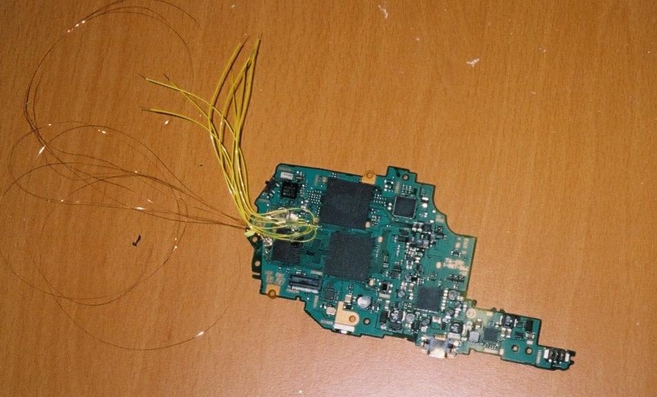
Now I just need to find the time and energy to finish my vhdl nand-interface...Which could be a while :( |
|
| Back to top |
|
|
laichung
Joined: 06 May 2005
Posts: 123
|
| Posted: Mon Apr 10, 2006 4:12 pm Post subject: |
|
|
hi dear all , I read this from china PSP forum that they can now flash the chips , but after re-flash a 1.5 firmware into a 2.6 machine , they found that PSP cant read the UMD disc anymore and cant update the PSP too. (They think that there are some different in hardware between different version of PSP) You guys can try to read the image of the post if you dont understand chinese.
http://www.cngba.com/read.php?tid=16024501 |
|
| Back to top |
|
|
ryoko_no_usagi
Joined: 29 Nov 2005
Posts: 65
|
| Posted: Mon Apr 10, 2006 5:14 pm Post subject: |
|
|
| Did they rewrite the whole nand? I think some characteristics of the nand/psp might be stored in one place in the nand which means it might not be a good idea to blindly overwrite everything. According to Mathieulh, the official updater doesn't touch this area.... |
|
| Back to top |
|
|
laichung
Joined: 06 May 2005
Posts: 123
|
| Posted: Mon Apr 10, 2006 6:55 pm Post subject: |
|
|
They dont give any detail about how to flash/which programmer they use. They only said they are using same tech. like reading the cell phone chip to dump the whole chip and re-flash it into other.
Also they are now offering a testing flash of the chip in china, so I think this page is not fake. If they post more detail on newsgroup , I can translate it to here if I have time.
If there are some information about the hardware saved inside the chip (like xbox360) to prevent replacement of hardware , then how come those unofficial shop can replace the broke UMD drive / LCD?
| ryoko_no_usagi wrote: | | Did they rewrite the whole nand? I think some characteristics of the nand/psp might be stored in one place in the nand which means it might not be a good idea to blindly overwrite everything. According to Mathieulh, the official updater doesn't touch this area.... |
|
|
| Back to top |
|
|
laichung
Joined: 06 May 2005
Posts: 123
|
| Posted: Mon Apr 10, 2006 7:07 pm Post subject: |
|
|
| They pointed out one thing: if you upgrade PSP from 1.0 to 1.5 , or downgrade PSP from 2.0 to 1.5 using same 1.5 firmware file , the last section (they didnt said which area) of the dumped chip is totally different from each other. I dont know they test it with same machine or two different machine. |
|
| Back to top |
|
|
Mathieulh
Joined: 19 Oct 2005
Posts: 68
|
| Posted: Mon Apr 10, 2006 7:52 pm Post subject: |
|
|
I comfirm the updater ONLY "touches" the IPL, the flash0 and the flash1 areas.
Beside the "end" of the NAND (exclueding ECC) should be flash1 so no wonder it changes.... |
|
| Back to top |
|
|
shifty
Joined: 16 Jun 2005
Posts: 32
Location: MIT
|
| Posted: Wed Apr 12, 2006 4:36 am Post subject: invalid blocks |
|
|
I believe it is unwise to completely recreate the entire chip from another, because you'll lose the invalid block information on your own flash.
if you lose the invalid block information on your own flash, you might
write to a bad block. all bets are off, then.
2013 of 2048 blocks are guaranteed, and the first block is guaranteed, so you have a 2012/2047 (98.29%) change of hitting a good block each time.
If your code is 40 blocks in size, you may have a 50-50 chance of having a good duplicate. (98.29^40=.501). Perhaps this is how they lost UMD capability?
I think what you have to do is e.g. copy all valid blocks to a file,
then check which blocks are valid in the new chip, and copy source
blocks to valid dest blocks.
page 11 of http://hitmen.c02.at/files/docs/psp/ds_k9f5608u0b_rev13.pdf
talks about the invalid blocks, but i honestly can't understand how to detect them....is it the 6th byte in the spare area? or the non FF data in column 517? (Or are they same??) |
|
| Back to top |
|
|
ryoko_no_usagi
Joined: 29 Nov 2005
Posts: 65
|
| Posted: Wed Apr 12, 2006 5:00 am Post subject: |
|
|
Yes of course block-mapping must be considered. And yes the 6th byte of the spare area identifies an initial invalid block if it's different from 0xff.
I would hope they write more intelligently than simply copy bit-for-bit. I would expect more disasterous results from bad blocks otherwise.
However, there is a special area in the nand that is used to store low-level settings. The UMD driver (and others) definitely touches this, but what exactly the use of this is remains unclear to me at this point. I'm investigating though :)
I can also reveal that the PSP crypto hw is involved as well... |
|
| Back to top |
|
|
dot_blank

Joined: 28 Sep 2005
Posts: 498
Location: Brasil
|
| Posted: Wed Apr 12, 2006 8:59 am Post subject: |
|
|
what can you reveal about the psp crypto hardware
can you post info or pm me info that you might have
_________________
10011011 00101010 11010111 10001001 10111010 |
|
| Back to top |
|
|
ryoko_no_usagi
Joined: 29 Nov 2005
Posts: 65
|
| Posted: Wed Apr 12, 2006 3:09 pm Post subject: |
|
|
| Not much more than what I wrote. I have seen opcode 18 used to manipulate data taken from that nand area. That's about all I currently know... |
|
| Back to top |
|
|
nem
Joined: 13 Jan 2005
Posts: 73
|
|
| Back to top |
|
|
ryoko_no_usagi
Joined: 29 Nov 2005
Posts: 65
|
| Posted: Wed Apr 19, 2006 7:43 pm Post subject: |
|
|
Cool work Nem! I think the board could use a little more glue though ;)
I wanna get back into the hardware-side myself...
By the way, dot_blank and other interested parties, opcode 18 appears to be an integrity/signature check. |
|
| Back to top |
|
|
Mathieulh
Joined: 19 Oct 2005
Posts: 68
|
| Posted: Thu Apr 20, 2006 1:32 am Post subject: |
|
|
Wow ! That's what I call a real mess ! xD
It must have taken hours to tear appart that poor psp mobo and wire it all the way.
By the way Nem, do you think it could be possible for you to dump the psp's ram at startup while running the 2.60 IPL so you could decrypt the 2.60 IPL and retrieve the new prx keys ?
If so it would be great especially as the very same protection will be embebed within the 3.00 IPL. |
|
| Back to top |
|
|
|

 FAQ
FAQ Search
 Memberlist
 Usergroups
 Register
 Profile
 Log in to check your private messages
 Log in


