| View previous topic :: View next topic |
| Author |
Message |
pyrosama
Joined: 13 May 2005
Posts: 66
|
 Posted: Tue Dec 13, 2005 5:39 am Post subject: Posted: Tue Dec 13, 2005 5:39 am Post subject: |
 |
|
I supose I could call them and ask if I can send my psp back after it quit working and send them a nice box of chips :P
When they dont send them back call and bitch demanding they replace it!
On a more serious note:
Are there any other chips you would like removed and photographed? The board is far gone now so it wont be any further hard :P
Canti_ |
|
| Back to top |
|
 |
Dr. Vegetable
Joined: 14 Nov 2005
Posts: 171
Location: Boston, Massachusetts
|
| Posted: Tue Dec 13, 2005 7:07 am Post subject: |
|
|
Yeah, they might conclude that you've voided your warranty. Unless you can convince them that this happened when you upgraded the firmware to 2.60...
RE: Pulling up chips, I think you got the important ones.
By the way, I just counted the layers on the main PC board. There are no fewer than eight levels of traces, and plenty of blind VIAs. There may be limits to what we will learn by visual inspection alone... |
|
| Back to top |
|
|
pyrosama
Joined: 13 May 2005
Posts: 66
|
| Posted: Tue Dec 13, 2005 8:56 am Post subject: |
|
|
If I can find easy way I want to sand board down layer by layer and scan pcb and digitize in cad.
Get full view of every thing.
(Any ideas of how to sand downlayers without sanding too far too fast?)
Canti_ |
|
| Back to top |
|
|
Dr. Vegetable
Joined: 14 Nov 2005
Posts: 171
Location: Boston, Massachusetts
|
| Posted: Tue Dec 13, 2005 9:07 am Post subject: |
|
|
Hmm... I've considered doing something like this myself, but I am sure it would be a HUGE effort and not very likely to work. I thought about peeling up some of the ground planes to see if I could make out what is going on underneath, but that was when I thought there might be only 4 or 5 layers total. It would probably be more productive (and a lot quicker) to use a continuity tester to try to figure out where some of the test points and other signal lines go.
I am also planning to "explode" a PSP in order to probe it while it is running. This is probably the only way we will figure out what some of these test points are for. |
|
| Back to top |
|
|
dot_blank

Joined: 28 Sep 2005
Posts: 498
Location: Brasil
|
| Posted: Tue Dec 13, 2005 9:40 am Post subject: |
|
|
thanks pyro for the pics again :) !!
and to lighten your bandwidth
here is a mirror with single zip archive
with all aforementioned cpu pics
great job ....hehe and that nand
area looks mighty toasty ;)
Download Zip
_________________
10011011 00101010 11010111 10001001 10111010 |
|
| Back to top |
|
|
HaQue
Joined: 25 Nov 2005
Posts: 91
Location: Adelaide, Australia
|
| Posted: Tue Dec 13, 2005 9:46 am Post subject: |
|
|
Do you have the wireless module to photograph in the great detail as you did the mainboard? Im wondering how the mainboard and module communicate.
At the risk of beating this to death, Im still after some good images of it.
Whats the possibility of removing the wireless model and making a different module to do other useful functions? I highly doubt it is like a minipci interface, but it could be possible to use the header on the mainboard for some other function.
This would probably be impossible with current firmware anyway.
_________________
www.smartwave-wireless.com |
|
| Back to top |
|
|
Dr. Vegetable
Joined: 14 Nov 2005
Posts: 171
Location: Boston, Massachusetts
|
| Posted: Tue Dec 13, 2005 10:57 am Post subject: |
|
|
I never did get back to figuring out how to upload pictures from my HandyCam, but if I do I'll try to post some pictures soon.
The shield on the WiFi module has a lid that snaps on/off, and a frame that is soldered to the board. Unfortunately, the frame has a support piece across the middle that seems to be designed to hide a lot of the good stuff. I had to really look around in there just to get the part number off the second chip. I think that you won't get much info from a picture unless we de-solder the frame.
Still, a picture is worth a thousand words, so I'll see what I can do. |
|
| Back to top |
|
|
dot_blank
Joined: 28 Sep 2005
Posts: 498
Location: Brasil
|
| Posted: Tue Dec 13, 2005 11:42 am Post subject: |
|
|
I will be sending my useless
daughter on over to pyros house for
some good RandR ;) hehe
and he will take very good pics for
us all and we will be happy and hopefully
this helps you guys out with wifi woahs :)
pyro: take a very good care of the skank ;)
and please do use a light blueish purplelish
light source as her eyes are very sensitive :P
i think this will make pics look extra sexy
cheers
_________________
10011011 00101010 11010111 10001001 10111010 |
|
| Back to top |
|
|
pyrosama
Joined: 13 May 2005
Posts: 66
|
| Posted: Tue Dec 13, 2005 3:57 pm Post subject: |
|
|
Hmm light blueish purplelish light source... I need to buy some purple shrink wrap and put on my flashlight (light source :P )
What is easiest method to remove the frame cleanly? My solder skills are poor at best.
Dot when are you planning on shipping out the dboard?
Canti_ |
|
| Back to top |
|
|
Dr. Vegetable
Joined: 14 Nov 2005
Posts: 171
Location: Boston, Massachusetts
|
| Posted: Tue Dec 13, 2005 10:45 pm Post subject: |
|
|
I am not sure what will be the best way to remove the frame. It is pretty small, and connected to the board very close to many of the components beneath, soldered at several tabs most of the way around the base.
Normally, I use stuff called Dry Wick ("DriWick?") which is a roll of copper braid. You simply hold the DryWick against a solder joint, heat with an iron, and the hot solder gets soaked up into the braid. If I don't have any wick handy, sometimes I just heat the joints and then quickly whack the board against a flat surface to get the hot solder to splatter off of the board. Most technicians that I know will also use a pair of cutters to separate the shield into smaller pieces, then pull them up individually. You might even just be able to heat the shield with a hot iron and pry it up.
Of course, since you stated that you lost your iron, none of this will help. This might be a bit delicate for that butane torch... |
|
| Back to top |
|
|
HaQue
Joined: 25 Nov 2005
Posts: 91
Location: Adelaide, Australia
|
| Posted: Wed Dec 14, 2005 9:54 am Post subject: |
|
|
I have removed the sheilds of many wireless card for modification,and I use a fine tipped soldering iron along with a solder sucker. For those that don't know what a solder sucker is, it is a spring loaded device that has small nozzle. You push the cener suction rod down and it locks in place. heat up the solder and hold the nozzle close. When the solder is liquid, press the button and the solder gets sucked up into the sucker.
You have to use one to appreciate how well it works. Ive fould it works alot better, and cleaner than solder wick. They are pretty cheap, Mine was approx AU$10(US$7).
For heating solder in very fine places, I wrap copper wire around the soldering iron tip and if need be, sharpen it as well.
Hope this helps someone.
HaQue
_________________
www.smartwave-wireless.com |
|
| Back to top |
|
|
Zenurb
Joined: 30 Sep 2005
Posts: 106
Location: United Kingdom
|
| Posted: Wed Dec 14, 2005 11:41 am Post subject: |
|
|
| HaQue wrote: | I have removed the sheilds of many wireless card for modification,and I use a fine tipped soldering iron along with a solder sucker. For those that don't know what a solder sucker is, it is a spring loaded device that has small nozzle. You push the cener suction rod down and it locks in place. heat up the solder and hold the nozzle close. When the solder is liquid, press the button and the solder gets sucked up into the sucker.
You have to use one to appreciate how well it works. Ive fould it works alot better, and cleaner than solder wick. They are pretty cheap, Mine was approx AU$10(US$7).
For heating solder in very fine places, I wrap copper wire around the soldering iron tip and if need be, sharpen it as well.
Hope this helps someone.
HaQue |
Solder suckers rule. They remind me of year 10 electronics class :D
_________________
Proud Dvorak User
US 1.5 PSP (Original) |
|
| Back to top |
|
|
digihoe
Joined: 14 May 2005
Posts: 108
|
| Posted: Wed Dec 14, 2005 1:37 pm Post subject: |
|
|
| Zenurb wrote: | | Solder suckers rule. They remind me of year 10 electronics class :D |
Too bad they break so easily... If you want you can also use a modified "dustsucker" (vacuum cleaner with a small straw), I find this more easy...
Best regards! |
|
| Back to top |
|
|
dot_blank
Joined: 28 Sep 2005
Posts: 498
Location: Brasil
|
| Posted: Wed Dec 14, 2005 2:36 pm Post subject: |
|
|
If we talk about hardware, especially with
electronics ....i would say most would know
what a soldersucker is ;)
unfortunately for pyro there is no
scorchersucker ...damn your really
nuts ;)
as for the board:
boxed and ready for address
will contact briefly for further
instructions
_________________
10011011 00101010 11010111 10001001 10111010 |
|
| Back to top |
|
|
Dr. Vegetable
Joined: 14 Nov 2005
Posts: 171
Location: Boston, Massachusetts
|
| Posted: Wed Dec 14, 2005 11:56 pm Post subject: |
|
|
| Not only do I know what a solder-sucker is, I even forgot what a solder-sucker is! I'm probably dating myself, but back when I learned how to solder, you used to be able to actually see the components with the naked eye... |
|
| Back to top |
|
|
pyrosama
Joined: 13 May 2005
Posts: 66
|
| Posted: Sat Dec 17, 2005 7:24 am Post subject: |
|
|
Photo's have been uploaded check them out!
Also these are the ground points of the connector to the dboard:
G G
| | | | | | | | | | | | | | | | | | | |
| | | | | | | | | | | | | | | | | | | |
G G G
As for the rest of them I dont have what it takes to find any thing else out about them I build a little continuity tester with an led and my HP 6203B DC Power Supply (fancy eq to play with leds :P ) however it will be prone to misleading me as it will not indicate if there is any resistance so small resistance would yield the same results as continuity.
Canti_ |
|
| Back to top |
|
|
Dr. Vegetable
Joined: 14 Nov 2005
Posts: 171
Location: Boston, Massachusetts
|
| Posted: Sun Dec 18, 2005 9:00 pm Post subject: |
|
|
| nem wrote: |
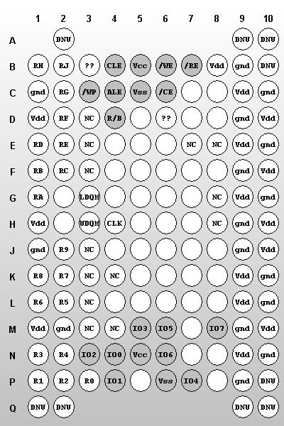
You would better to add power pads for flash,
| Code: |
Vss Power ground for flash chip
Vcc +3.3V power for flash chip
|
GND and Vdd is for DRAM. Vcc(+3.3V) is used for some I/O including daughter board.
|
Ok, I finally updated the pinout to reflect these corrections. The grey pins are the ones that are used for flashing the chip:
 |
|
| Back to top |
|
|
Dibblah
Joined: 03 Nov 2005
Posts: 13
|
| Posted: Mon Dec 19, 2005 7:52 am Post subject: |
|
|
So now we have all flash pins identified as externally accessible. What stops us from cutting the tracks (possibly /CE and /WE only), chemically stripping the enamel off them and soldering on our own board with a http://www.samsung.com/Products/Semiconductor/NANDFlash/SLC_SmallBlock/256Mbit/K9F5608U0D/ds_k9f5608x0d_rev03.pdf?
edit - Hmmm... Looks like the data bus is not tri-stated when CE is inactive :(
I really don't see that hot-swapping can possibly work - For a start, the bad blocks list is likely to be cached, etc. So the NAND'd have to be prewritten.
Cheers,
Allan. |
|
| Back to top |
|
|
digihoe
Joined: 14 May 2005
Posts: 108
|
| Posted: Mon Dec 19, 2005 11:02 am Post subject: |
|
|
Yes yes... With all the flashpoints needed, atleast external programing should work... Anyone tried it?
What kind of flasher would be needed to externally flash it? Also do one need to write a program to be able to read/write the chip, nem indicates that...
Best regards and hope external programming will be with us in the future. |
|
| Back to top |
|
|
Dr. Vegetable
Joined: 14 Nov 2005
Posts: 171
Location: Boston, Massachusetts
|
| Posted: Mon Dec 19, 2005 4:38 pm Post subject: |
|
|
Hot-swapping does seem like a long shot. But then again, PSP homebrew was considered to be a long shot not so long ago.
It might be possible to flash two chips so that they have the same list of bad blocks, but you would essentially have to mark both chips with the union of both sets of bad blocks. On a wing and a prayer, this might work until new bad blocks develop on either chip, but that also assumes that you can re-flash the original one in the first place, which is the "crux of the biscuit", to borrow from Frank Zappa.
That doesn't rule out cold swapping, though...
As far as external flashing goes, nobody has yet figured out how to get to these lines without opening the case and/or cutting traces, so we're still probably a long way away from that. |
|
| Back to top |
|
|
Dibblah
Joined: 03 Nov 2005
Posts: 13
|
| Posted: Mon Dec 19, 2005 6:45 pm Post subject: |
|
|
Am I misunderstanding this, or is SmartMedia just a direct access NAND flash chip?
Surely a flasher can't be as simple as just a $20 USB card reader and wiring up a dummy smartmedia card to the traces already identified...?
http://elm-chan.org/docs/sm_e.html
And the NAND flash could also be harvested off a SM card, for dual use (Yes, it's a lot large, and you need a 32Mb card rather than 64, which probably won't work due to protocol changes)
Cheers,
Allan.
Last edited by Dibblah on Mon Dec 19, 2005 6:55 pm; edited 1 time in total |
|
| Back to top |
|
|
Dibblah
Joined: 03 Nov 2005
Posts: 13
|
| Posted: Mon Dec 19, 2005 6:47 pm Post subject: |
|
|
| Dr. Vegetable wrote: |
As far as external flashing goes, nobody has yet figured out how to get to these lines without opening the case and/or cutting traces, so we're still probably a long way away from that. |
What's wrong with opening it and cutting traces?
If it's a brick anyway... :)
Cheers,
Allan. |
|
| Back to top |
|
|
user303
Joined: 15 Dec 2005
Posts: 2
|
| Posted: Mon Dec 19, 2005 9:06 pm Post subject: |
|
|
this is 100% speculation but still:
Sony must have thought about some way to repair bricked psp's.
With millions units sold and the high frequency of new firmwareupgrades there must be some percentage that the legal firmware upgrades go wrong.
Even with 0.1% failure rate, these bricked units have to be in some way easily repairable, as these units get sent in for repair.
Atleast in my mind it would make sense ;)
So keep up the excellent work! |
|
| Back to top |
|
|
digihoe
Joined: 14 May 2005
Posts: 108
|
| Posted: Mon Dec 19, 2005 9:21 pm Post subject: |
|
|
| Dibblah wrote: | | Dr. Vegetable wrote: |
As far as external flashing goes, nobody has yet figured out how to get to these lines without opening the case and/or cutting traces, so we're still probably a long way away from that. |
What's wrong with opening it and cutting traces?
If it's a brick anyway... :)
Cheers,
Allan. |
Agreed. If you think it would happen again (brick) maybe you could add a small special made connector...
| user303 wrote: | this is 100% speculation but still:
Sony must have thought about some way to repair bricked psp's.
With millions units sold and the high frequency of new firmwareupgrades there must be some percentage that the legal firmware upgrades go wrong.
Even with 0.1% failure rate, these bricked units have to be in some way easily repairable, as these units get sent in for repair.
Atleast in my mind it would make sense ;) |
Sure, there is most certainly a way but since we don't know about it making an own interface is the best way to go... A SONY protocol could use bootstraps that are encoded with the privatekey (if it is some kind of JTAG stuff) or even worse they could have made a new protocol that noone knowes about (SONY like to do stuff thier way)...
Since we're speculationg, I heard roumors about the IPL that this contains a way in to the flash...
Best regards and keep up the great work! |
|
| Back to top |
|
|
digihoe
Joined: 14 May 2005
Posts: 108
|
| Posted: Mon Dec 19, 2005 9:26 pm Post subject: |
|
|
| Dibblah wrote: | Am I misunderstanding this, or is SmartMedia just a direct access NAND flash chip?
Surely a flasher can't be as simple as just a $20 USB card reader and wiring up a dummy smartmedia card to the traces already identified...?
http://elm-chan.org/docs/sm_e.html
And the NAND flash could also be harvested off a SM card, for dual use (Yes, it's a lot large, and you need a 32Mb card rather than 64, which probably won't work due to protocol changes)
Cheers,
Allan. |
I like how you think! Maybe this could work, but I'm sure there is some ID for the chip etc. that need to be considered. With a "homemade" application this might just work (would be rather nice)... |
|
| Back to top |
|
|
Dr. Vegetable
Joined: 14 Nov 2005
Posts: 171
Location: Boston, Massachusetts
|
| Posted: Mon Dec 19, 2005 10:21 pm Post subject: |
|
|
| Dibblah wrote: | | What's wrong with opening it and cutting traces? |
Nothing wrong with that at all, but that's not what I would call "external" flashing. Those traces are pretty darn small, so I hope you know a good brain surgeon... The ultimate goal is to be able to move freely between firmware versions without opening the case or having wires dangling outside.
| digihoe wrote: | | I heard roumors about the IPL that this contains a way in to the flash... |
Actually, any PSP application has access to the flash through the sceNand functions, but nobody has figured out how these work yet. (This is how the firmware upgrade programs work.) Doing that will require some trial and error, but each "error" will result in a nice shiny brick. This is the primary motivation for figuring out how to re-flash a dead PSP.
| Dibblah wrote: | | Am I misunderstanding this, or is SmartMedia just a direct access NAND flash chip? Surely a flasher can't be as simple as just a $20 USB card reader and wiring up a dummy smartmedia card to the traces already identified...? |
I had a similar idea. (Great link, BTW!) This will probably require custom software to write the proper format to the stick, but that might be all the hardware one would need. |
|
| Back to top |
|
|
Dibblah
Joined: 03 Nov 2005
Posts: 13
|
| Posted: Tue Dec 20, 2005 7:45 am Post subject: |
|
|
| Dr. Vegetable wrote: |
| Dibblah wrote: | | Am I misunderstanding this, or is SmartMedia just a direct access NAND flash chip? Surely a flasher can't be as simple as just a $20 USB card reader and wiring up a dummy smartmedia card to the traces already identified...? |
I had a similar idea. (Great link, BTW!) This will probably require custom software to write the proper format to the stick, but that might be all the hardware one would need. |
Shouldn't need to. Linux should do this almost natively.
Cheers,
Allan. |
|
| Back to top |
|
|
Dr. Vegetable
Joined: 14 Nov 2005
Posts: 171
Location: Boston, Massachusetts
|
| Posted: Tue Dec 20, 2005 8:06 am Post subject: |
|
|
How would that work? (Not doubting that it would, just intensely curious.)
The flash chip in the PSP has three distinct regions that would need to be programmed. Would these appear as separate partitions? I was under the impression that a regular SM card would only present a single partition to the host computer. |
|
| Back to top |
|
|
Dibblah
Joined: 03 Nov 2005
Posts: 13
|
| Posted: Tue Dec 20, 2005 8:43 am Post subject: |
|
|
| Dr. Vegetable wrote: | How would that work? (Not doubting that it would, just intensely curious.)
The flash chip in the PSP has three distinct regions that would need to be programmed. Would these appear as separate partitions? I was under the impression that a regular SM card would only present a single partition to the host computer. |
Easiest option:
dd if=/dev/sda1 of=pspdump
mount -t fat -o loop,offset=1234 ./pspdump /mnt/pspflash
<change whatever>
umount /mnt/pspflash
dd if=./pspdump of=/dev/sda1
This assumes that your reader shows each device as a "partition" under linux - Which most do. Obviously, offset is incorrect and would have to be discovered. But since fat has a nice string at the beginning, this shouldn't be too hard.
Cheers,
Allan. |
|
| Back to top |
|
|
Dr. Vegetable
Joined: 14 Nov 2005
Posts: 171
Location: Boston, Massachusetts
|
| Posted: Tue Dec 20, 2005 8:58 am Post subject: |
|
|
Well if that would work then it seems like you could cut the traces going to the flash and connect them instead to an SM slot. Then program a different SM card with each firmware version and swap versions simply by swapping SM cards. Of course, the RAM control lines would stay connected to the original chip. You could possibly even retain the ability to use the original flash simply by wiring the chip selects through a DPDT switch to select between the NAND and the SM card for booting.
Hmm...
EDIT:Changed "SD" to "SM", per digihoe's correction. Big difference between SecureDigital and SmartMedia cards. Too many freakin' form factors! (Thanks digi!)
Last edited by Dr. Vegetable on Tue Dec 20, 2005 10:14 am; edited 1 time in total |
|
| Back to top |
|
|
|

 FAQ
FAQ Search
 Memberlist
 Usergroups
 Register
 Profile
 Log in to check your private messages
 Log in


